
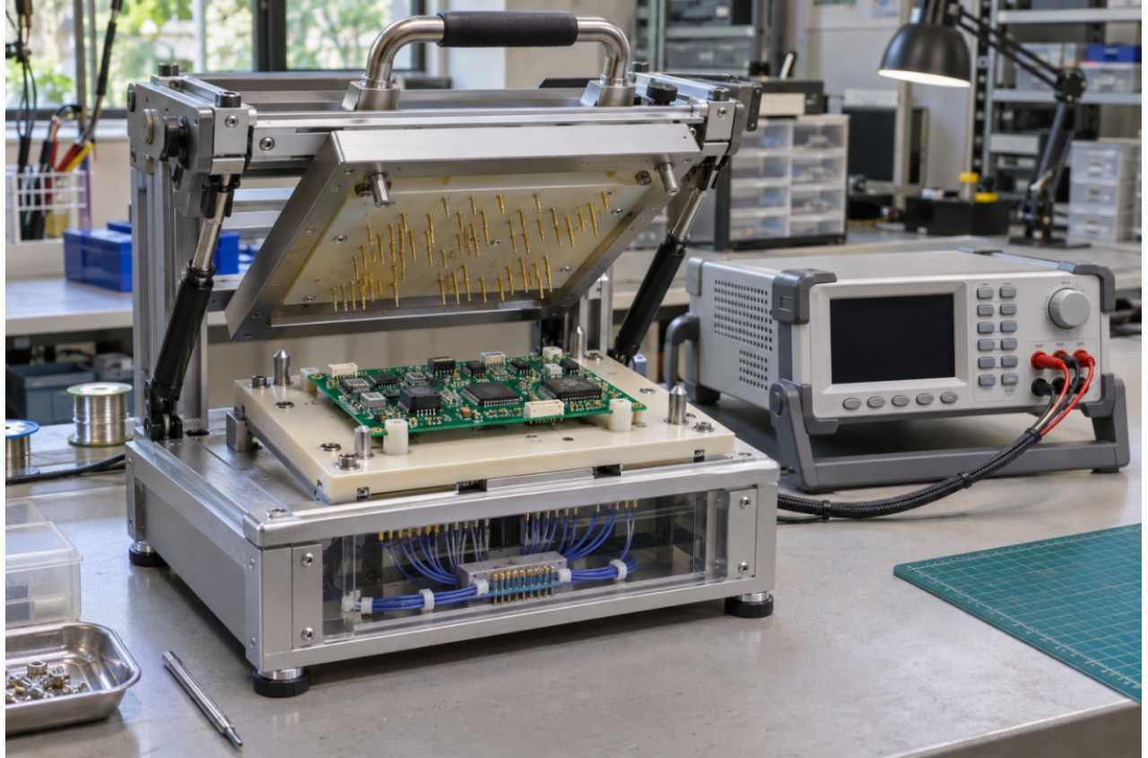
A PCB test fixture for contact resistance must do more than produce a stable reading. It must measure the intended connection, distinguish product variation from fixture variation, and repeat that measurement under production conditions. The design starts with a defined electrical boundary, then brings the probe layout, board support and measurement settings into agreement with it.
For manufacturers, that distinction affects both yield and troubleshooting. An unstable probe can send an acceptable board for unnecessary rework, while an unintended current path can conceal a defective connection. A well-specified PCB test fixture makes the result traceable to a particular board feature and a controlled test method.
Define the connection before choosing a PCB test fixture
Begin by deciding what “contact resistance” means for the product. A connector contact, a solder joint and a complete power path are different measurement targets. If the sense points span a connector, two solder joints and a length of PCB copper, the result represents that combined path. It cannot be reported as the resistance of the connector interface alone.
The PCB testing fixture’s own probe-to-pad contact is a separate concern. When measuring a board connection, the aim is usually to keep fixture contact losses outside the measured voltage span. When qualifying the probe interface itself, those losses become part of the test object. The same wiring arrangement cannot be assumed to answer both questions.
Mark the current path and voltage-sensing locations on the board drawing before assigning test points. Review the schematic for parallel paths that could divert current around the target joint. Four-wire sensing does not isolate a connection from the rest of the circuit. If the assembled board cannot provide a defined path, the test may require isolation, a different assembly stage or a dedicated coupon.
Use the required decision margin to determine where the PCB test fixture needs Kelvin access. There is no universal resistance value below which every net needs four-wire measurement. The relevant question is whether the expected lead and contact errors are acceptable relative to the product tolerance and the measurement uncertainty.
Carry the four-wire Kelvin connection to the intended boundary
A four-wire Kelvin test uses one pair of leads to force current and another to sense voltage. Because the voltage input draws very little current, the sense leads contribute little voltage drop. Separating these paths allows the instrument to exclude force-lead losses that a two-wire measurement would include. NI explains this distinction in its guidance on switching low-level signals to a DMM.
When configuring a Kelvin test fixture for a board-path measurement between locations A and B, provide independent force and sense access at both ends. Joining force and sense at a fixture connector leaves the shared conductor, probe and contact downstream of that junction within the measured path. Bringing separate sense contacts to the board establishes a more useful boundary for evaluating the product.
A four-wire test fixture can provide that access through separate probes or a purpose-built Kelvin probe with electrically independent contacts. Confirm the actual internal construction; two wires connected to one conventional probe do not create independent sensing at its tip. Draw the force and sense routes through the interface and any switching hardware so that maintenance staff can verify the complete connection.
Where two tips share a pad, position them according to the current flow and the feature being measured. Copper has a voltage gradient under load, so moving a sense point can change the result. Pad diameter alone does not establish whether that change is negligible. Review copper thickness, geometry and placement tolerance, then validate the proposed locations against the required measurement margin.
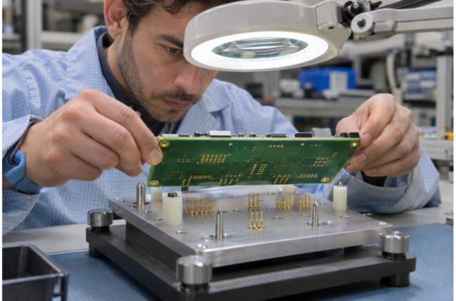
Match probe access and board support to the PCB
Build the PCB test fixture from controlled board data. The netlist and fabrication files establish the electrical layout, while assembly information identifies component heights, access restrictions and mechanical references. Reconcile these with the approved test-point list and PCB revision. A copper feature that appears accessible in CAD may be covered by solder mask or obstructed on the assembled board.
Review representative physical boards before releasing the circuit board test fixture for manufacture. Surface finish, solder shape and residue can change how a tip lands, and manufacturing tolerances affect how much usable contact area remains. A probe selection that works on one clean sample still needs evaluation across the board variation expected in production.
Select tip geometry, spring force and working travel together. The probe must establish reliable contact without damaging the pad or overstressing the assembly. Use the selected model’s specifications rather than a generic force or resistance target. Set PCB test fixture closure to achieve the specified working travel across the expected board tolerances, without exceeding the probe’s maximum stroke.
When selecting actuation for a PCB testing fixture, assess vacuum and guided pressing against board geometry, access and total loading. Neither is automatically the correct choice for a particular board size. Position supports to control deflection around the probed areas, while avoiding components and sensitive features. Verify the resulting travel across board thickness and warp tolerances instead of relying only on the nominal plate dimensions.
Specify test conditions before setting the production limit
The PCB test fixture specification should define the board’s electrical state as clearly as its connections. Perform resistance measurements with the assembly in the state required by the approved method, normally unpowered and discharged. Consider whether the applied stimulus could forward-bias semiconductor paths or alter the contact being evaluated.
Choose test current to obtain a usable signal without unacceptable heating or contact modification. A current range suitable for one connector or copper path is not a general production setting. Where the objective is to evaluate an undisturbed contact film, use the applicable low-level or dry-circuit method. Keithley describes dry-circuit testing as typically limiting voltage across the device to 20 mV or less; the required current and open-circuit limits must also be checked against the governing method and instrument configuration. See the Low Level Measurements Handbook, Section 3.3.5.
Establish measurement timing after the Kelvin test fixture has engaged and switching has settled. Evaluate representative boards and stations rather than selecting a delay from one stable sample. The chosen integration time and any averaging must support the required discrimination within the available cycle time. Averaging should not conceal intermittent contact or replace investigation of unstable readings.
In a four-wire test fixture, thermoelectric offsets can become significant when the measured signal is small. Current reversal or offset-compensated measurement can reduce their contribution, provided the instrument and board support the method and the offset remains sufficiently stable during the sequence. These techniques do not correct an incorrect sensing boundary or unwanted parallel path. Their operating conditions are discussed in Section 3.3 of the Keithley handbook cited above.
Set the acceptance limit from the product’s electrical, thermal and reliability requirements. Production data then helps assess process capability and whether the measurement system can support that limit. A sample distribution alone cannot establish what the product is allowed to pass. Include temperature effects and measurement uncertainty in the decision rule, especially when readings approach the specification boundary.
Validate PCB test fixture accuracy and repeatability separately
A calibrated low-resistance reference can check the instrument and routed measurement chain, but it does not reproduce every feature of a probe landing on a production board. Use a suitable reference or coupon to establish electrical correlation, then evaluate repeated loading of representative assemblies to assess the contact and positioning process.
Repeated readings without reopening the PCB test fixture mainly show short-term electrical stability. Removing and reinserting the board introduces the mechanical variation that production actually experiences. Extend the study across relevant stations, board samples and loading conditions so that a favorable result from one nest does not stand in for the entire system.
Compare circuit board test fixture results with a suitable reference measurement using equivalent sense locations and test conditions. Otherwise, a difference may reflect two measurement definitions rather than fixture error. Include controlled challenges near the acceptance boundary and verified fault conditions where practical. A known-good board alone cannot demonstrate that the system rejects the intended defect.
Agree PCB testing fixture acceptance criteria before running the study. Sample size, allowable bias, repeatability and reference-check frequency should follow the product risk and quality requirements. Fixed rules such as “30 insertions” or “one-third of the limit” are not substitutes for that assessment. Keep the approved wiring drawing, settings and validation results together so that later changes can be evaluated against the original measurement definition.

Maintain the measurement when moving into automated testing
Automation makes PCB test fixture engagement and test sequencing repeatable, but the measurement still depends on the installed probes, instruments and program. Preserve the validated sensing locations when transferring a bench method to an automated station. Where several nests run in parallel, establish correlation between them and retain station identity with the results.
Jettest’s Fully Automatic PCBA ICT/FCT Test System supports automated in-circuit testing and functional testing with dual- or multiple-station arrangements and compatibility with different fixtures. For contact resistance measurement, the required Kelvin connections, instrument range, switching arrangement and acceptance method need project-specific confirmation. The platform description does not by itself establish a low-resistance accuracy specification.
PCB test fixture maintenance should respond to contact performance as well as usage. Record insertion counts, cleaning and probe replacement, then compare reference readings before and after intervention. A reference board also needs controlled handling and periodic verification because its pads and contacts can change with use. Investigation should distinguish a fixture-related shift from an actual change in the production boards.
Questions to resolve before fixture release
Can two probes share one pad for a Kelvin connection
Yes, if the pad provides reliable independent access and the contact locations match the intended measurement boundary. Validate landing tolerance, probe travel and the effect of current flow across the pad. A nominally large enough pad does not guarantee a repeatable result.
What probe resistance should trigger maintenance
Use the selected probe’s specification and the validated fixture baseline. Probe internal resistance, probe-to-pad contact resistance and measured board-path resistance are different quantities. A universal alarm such as 100 mΩ can be inappropriate for both the hardware and the product decision.
What information should a PCB test fixture supplier receive
For a custom PCB testing fixture, provide controlled PCB and assembly data together with a marked drawing of the target connection and sense locations. The supplier also needs the product acceptance requirement, permitted stimulus and expected production conditions to evaluate the measurement chain and mechanics. To discuss integration into an automated station, contact Jettest about your PCBA test requirements with those inputs and the intended cycle time.